Printed Circuit Boards (PCBs) form the backbone of major electronics. These awesome creations pop up in most computational electronic equipment, such as simpler devices such as digital clocks, calculators etc.
For the uninitiated, a PCB paths electric signals through electronic equipment, which suits the device’s mechanical and electrical circuit demands. Simply speaking, PCBs inform the power where to proceed, bringing your electronic equipment .
PCBs directly present around their face by means of a network of aluminum pathways. The intricate method of aluminum routes determines the special purpose of every piece of printed circuit board. Also check– PCB box supplier
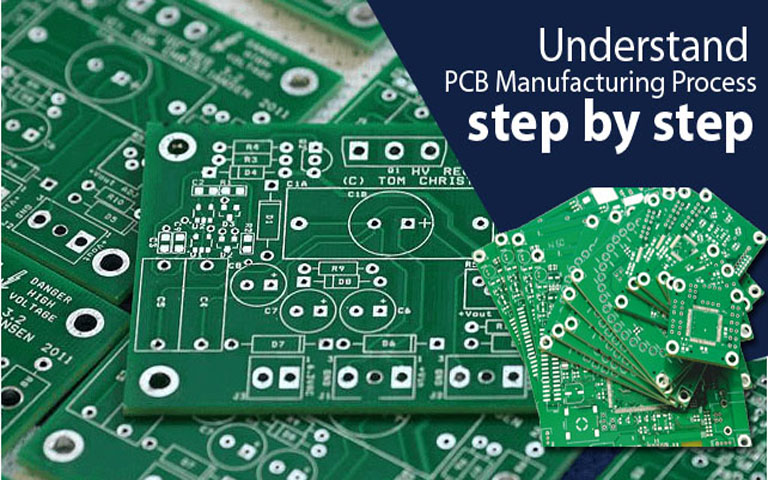
PCB Manufacturing Procedure Steps
Step 1: Layout and Output
Circuit boards ought to be rigorously harmonious with a PCB design produced by the designer using PCB design program . Commonly-used PCB manufacturing and assembly design software comprises Altium Designer, OrCAD, Pads, KiCad, Eagle etc..
Step 2: From Document to Film
PCB printing starts later, designers output PCB schematic documents and producers run a DFM check. Manufacturers utilize a unique printer known as a plotter, making picture films of their PCBs, to publish circuit boards.
Step 3: Printing the Internal layers: Where Can the Copper Move?
The creation of movies in the preceding step intends to map out a figure of aluminum path. Now it is time to publish the figure over the movie on a copper foil.
This measure in PCB manufacturing prepares to create real PCB. The fundamental kind of PCB includes a laminate plank whose center material is epoxy resin and glass fiber which are also referred to as substrate material.
Step 4: Removing the Unwanted Copper
Together with the photoresist removed along with the tempered resist covering the aluminum we wish to maintain the board proceeds into the next phase: unwanted aluminum removal. As the alkaline solution eliminates the resist, a more potent chemical preparation eats off the extra aluminum.
Step 5: Layer Alignment and Optical Inspection
Considering all the layers tidy and prepared, the layers need alignment punches to make sure that they line up. The enrollment holes align with the internal layers to the outside ones. The technician puts the layers into a system known as the optical punch, which allows an specific correspondence so that the registration holes are correctly punched.
Step 6: Layer-up and Bond
Within this phase, the circuit board takes shape. Each of the separate layers anticipate their marriage . Together with the layers prepared and verified, they just should fuse together. Outer layers must combine together with the substrate. The procedure occurs in two steps: layer-up and bonding.
Step 7: Drill
At length, holes are drilled to the heap plank. All elements slated to come after, for example copper-linking through holes and leaded facets, rely upon the exactness of precision drill holes. The holes have been drilled into a hair’s-width – that the drill accomplishes 100 microns in diameter, whilst hair averages in 150 microns.
Step 8: Plating and Copper Deposition
After drilling, the panel goes onto plating. The procedure fuses the various layers together using compound residue. Following a thorough cleaning, the panel undergoes a series of chemical baths. Throughout the bathrooms, a compound residue process deposits a thin coating – about a micron thick – of aluminum across the surface of the panel.
Step 9: Outer Layer Imaging
In Step 3, we implemented photoresist into the panel. In this measure we do it – but this time we picture the outer layers of this panel together with PCB design. We start with the layers in a sterile room to avoid any contamination from sticking to the coating surface, then use a coating of photoresist into the panel.
Step 10: Plating
We return into the darkened room. As we did in Step 8we electroplate the plank using a thin coating of aluminum. The exposed parts of this panel in the outer coating photoresist stage get the aluminum electro-plating.
Step 11: Closing Etching
The tin protects the copper in this phase. The unwelcome exposed aluminum and aluminum beneath the residual resist layer experience elimination. Again, chemical alternatives are employed to eliminate the aluminum. The tin protects the appreciated copper in this phase.
Step 12: Solder Mask Program
Ahead of the solder mask is applied to either side of the plank, the panels have been cleaned and coated with an epoxy solder mask ink. The planks get a burst of UV light, which moves through a solder mask photograph picture.
Step 13: Surface End
To include extra solder-ability into the PCB, we plate them with silver or gold. Many PCBs also get hot air-leveled pads in this phase. The hot air leveling ends in uniform pads.
Step 14: Silkscreen
The nearly finished board receives ink-jet composing on its own surface, used to signify each of very important information of interest to the PCB. The PCB eventually passes onto the previous coating and healing stage.
Step 15: Electric Test
As a last precaution, a tech performs electric tests on the PCB. The automatic process confirms the performance of the PCB and its conformity to the initial layout.
Step 16: Profiling and V-Scoring
Now we have come to the previous step: trimming. Various boards are cut out of the first panel. The process employed either centers around using a router or even a v-groove. A router leaves little tabs across the plank edges whereas the v-groove cuts diagonal stations across either side of the plank.
The latest technology advancement is giving rise to more advanced PCB’s. I hope you like reading on PCB Manufacturing
