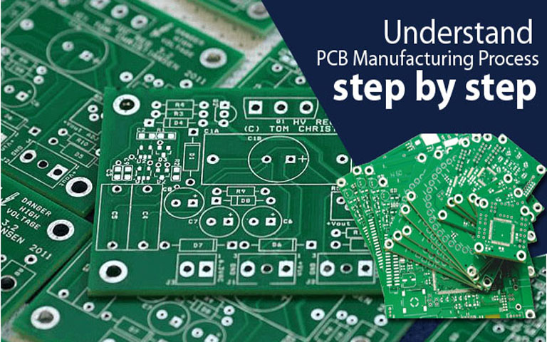
Understand PCB Manufacturing Process step by step
Printed Circuit Boards (PCBs) form the backbone of major electronics. These awesome creations pop up in most computational electronic equipment, such as simpler devices such as digital clocks, calculators etc.
For the uninitiated, a PCB paths electric signals through electronic equipment, which suits the device’s mechanical and electrical circuit demands. Simply speaking, PCBs inform the power where to proceed, bringing your electronic equipment .
PCBs directly present around their face by means of a network of aluminum pathways. The intricate method of aluminum routes determines the special purpose of every piece of printed circuit board. Also check– PCB box supplier
PCB Manufacturing Procedure Steps
Step 1: Layout and Output
Circuit boards ought to be rigorously harmonious with a PCB design produced by the designer using PCB design program . Commonly-used PCB manufacturing and assembly design software comprises Altium Designer, OrCAD, Pads, KiCad, Eagle etc..